
Washington Nanofabrication Facility

University of Washington
Washington Nanofabrication Facility
Mason Road Seattle, WA
The Washington Nanofabrication Facility (WNF) is an open-access, nanofabrication facility at the University of Washington. Lab users have access to fabrication tools and expert staff. The WNF specializes in MEMS, optics, and photonics, but is equipped for most micro- and nanofabrication needs.
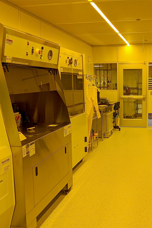
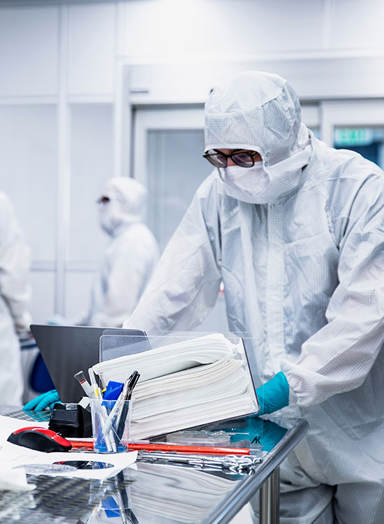
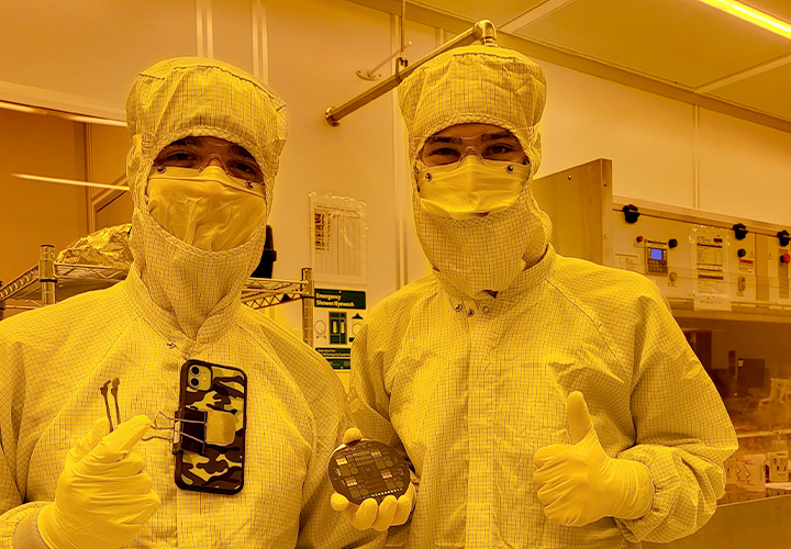
The Washington Nanofabrication Facility (WNF) consists of a 15,000-square-foot cleanroom space. The WNF focuses on MEMS, optics, and photonics and is available for academic and industrial use.
Facility at a Glance
- Facility type: University cleanroom, Shared user facility, Research laboratory, Teaching laboratory, Workforce training facility
- Facility mission: Education and training, Academic research, MEMS / microsystems development, Nanotechnology research
- Facility size: About 13,000 square feet including bays and chases. Bays are ISO 5, 6, and 7. 8 bays: wet etch, lithography, metrology, PVD and plasma etch, CVD and dry etch, teaching lab, electroplating, and back end/assembly.
- Cleanroom classification: ISO 5, ISO 6, ISO 7,
- Primary contact: Darick Baker, Acting Director
- Location: 115 Fluke Hall / 4000 Mason Road
Seattle, WA 98195 - Institution website: https://www.uw.edu/
- Facility website: https://www.wnf.uw.edu/
- Training program: https://www.wnf.uw.edu/education-outreach/
- Equipment and capabilities: https://www.coral.uw.edu/tools/?lab=WNF
Core Capabilities
Lithography
- Photolithography – Coat/Expose/Develop
- Maskless lithography / direct-write lithography
Etching and Material Removal
- Wet etching – KOH, BOE etc.
- Vapor Etching – HF Vapor and/or XeF2 for example
- Dry etching / RIE
- Deep reactive ion etching / DRIE
Packaging and Assembly
- Wafer bonding
- Packaging and wire bonding
Featured Equipment
- Microfluidics
- MEMS Sensor/Actuator fabrication
- Nanomaterials processing
Thin Films and Thermal Processing
- Thin film deposition – Sputter/Evap
- Thermal oxidation
Metrology and Electrical Characterization
- Metrology – Optical/SEM CD’s
- Metrology – Thin Film/Profilometry
- Electrical testing
Device Fabrication and Specialized Processing
- Microfluidics
- MEMS Sensor/Actuator fabrication
- Nanomaterials processing
Materials and Applications
Materials Commonly Processed
- Silicon
- Silicon Dioxide
- Silicon Nitride
- Metals
- Alloys
- III-V materials
- Glass
- Polymers
- Photoresists, SU8 etc.
- Nanomaterials
Devices and Application Areas
- MEMS Sensors
- MEMS Actuators
- Photonics / optoelectronics
- Microfluidics
- Quantum devices
- Sensors and transducers
- Thin film devices
- Educational demonstration devices
Metrology, Characterization, and Assembly
Metrology and Characterization
- Optical microscopy
- Profilometry
- Ellipsometry
- Film thickness measurement – Profilometry, Reflectometry
- SEM
- AFM
- Electrical Probing
- I-V / C-V testing
- Sheet Resistance
- Surface analysis (EDX, for example)
Packaging and Assembly
- Dicing
- Wire Bonding
- Probe Station Testing
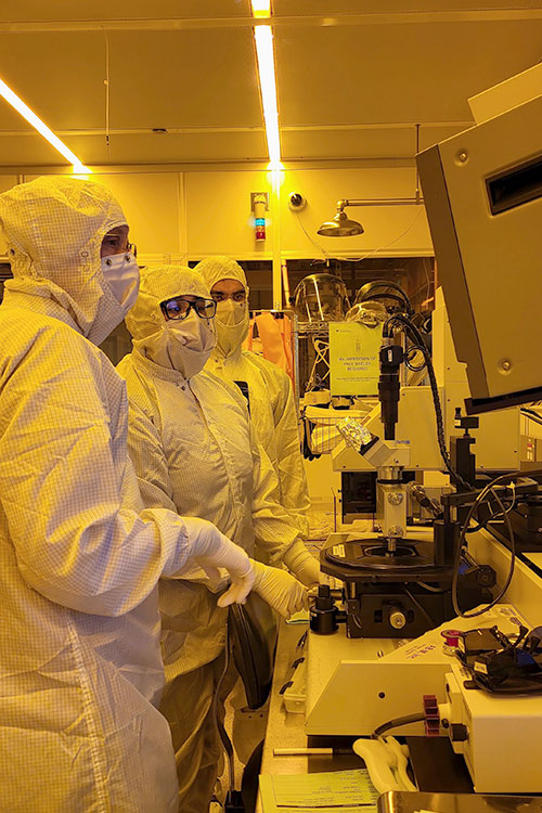
Education and Workforce Development
Training Offerings
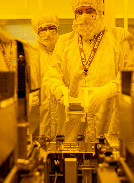
- Cleanroom safety training
- Tool-specific training
- Metrology training
- Short courses / bootcamps
Delivery formats: In-person, Short course, Semester course, Summer program
Courses and programs: EE527, EE331, 1-week fabrication short course, equipment repair short course (in development)
Approximate annual participation: 16 year-around interns, ~36 people through short courses per year, ~80 new users per year, ~100 students in EE331 and EE527
External or partner training: Yes
Instructional Resources
We run a Schottky Diode project that is very sharable–process flows, mask layout, etc.
Opportunities for Collaboration
- Shared training materials
- Faculty professional development
- Student exchanges or visits
- Shared process flows
- Equipment best practices
- Safety procedures
- Proposal development
- Workforce grant opportunities
- Conference presentations
- Outreach activities
Potential contribution to WaferWorkforce: We have a bunch of interns that I can put on projects
Resources or connections sought: Professional connections for staff–opportunities to discuss problems; shared process flows and tool processes
Accessing the Facility
External access or partner training status: Yes. Prospective collaborators should contact the facility directly to discuss access, training, visits, research, or workforce-development opportunities.
Contact:
Darick Baker
Acting Director
University of Washington
Email: [email protected]
Phone: 206-221-8265